Big Dumb Sequencer
- Dimensions
- 58 HP
- 22 mm deep
- Current Draw
- 20 mA +12V
- 6 mA -12V
- 0 mA 5V
- Price
- $415
Available as an assembled Module and as a DIY project.
This Module is currently available.
MG ID: 53762
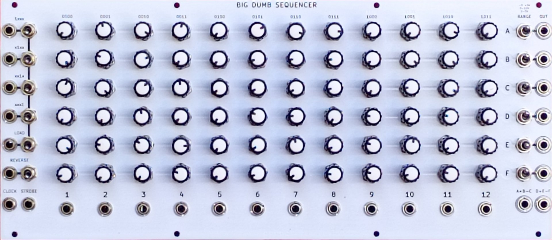
12-step, 6 channel binary addressable analogue step sequencer
12 step, 6 channel analogue step sequencer with binary addressing and clocked operation.
There are so many nice, compact, intuitive sequencer designs out there in eurorack packed with modern features that make performances easier and patches more repeatable.
This one is big and dumb.
Not just dumb in the sense that it is a silly 72-knob monster that eats up rack space and takes ages to build but mainly because it is all analogue and CMOS counters/logic.
No microcontrollers, no patch memory, no quantisation, no tap tempo.
Despite being so enormous it's actually very light on features and is intended to be patched with logic, LFOs, and counters/dividers to make more complex sequences. It doesn't even have an onboard clock source.
I specifically chose 12 steps over 16 because my system is already full of counters/dividers that naturally produce things in twos, fours, and eights.
If you're familiar with my Melakarta module you'll recognise a lot of the control circuit is reused/modified here.
My original plan was to make a gate/trigger sequencer for driving DAC/Melakarta and envelope generators using rows of toggle switches instead of potentiometers (still absolutely possible to use it this way, just turn unwanted steps to 0 and any step turned up is a gate!)
6 channels allows sequencing of every input of my DAC module, or sequencing the 3-bit addresses of two Melakartas.
Operation:
The left hand side of the module controls the sequencer, right side is the outputs.
The most basic way to use it is to set all the left side toggle switches down and patch a steady tempo to the CLOCK input.
The signal you use for CLOCK doesn't have to be a hard-edged gate or pulse, it'll convert any signal that crosses approx. 0.5V into a square.
On the rising edge of the signal on CLOCK the sequencer will advance to the next step until it reaches the end and then jumps to the position decided by the binary address bits.
0000 = 1, 0001 = 2, 0010 = 3, 0011 = 4 etc.
REVERSE (you guessed it) reverses the direction of clocking but also (importantly) inverts all 4 address bits.
REVERSE has a jack input and toggle switch.
This jack input, like all the left hand side jacks, converts anything above 0.5V to ON and below that to OFF.
The toggle switch inverts the logic of the input so with the switch down a gate enables REVERSE mode and with the switch up REVERSE is on until a gate turns it off. With nothing plugged in it works as a manual control for REVERSE.
LOAD also has a jack and toggle switch but this toggle switch works a little different to the other inputs.
With the switch down the current binary address is loaded once on the rising edge of the signal on the LOAD input (Think sample and hold but for a binary address).
Patching a gate output from one of the steps to LOAD can be used to set the length of a clocked sequence. Patch gate 9 to LOAD for an 8-step forward-clocked sequence, for example.
With the toggle switch up and nothing patched into the LOAD jack the sequencer will follow the binary address and ignore clocking.
With a signal plugged in and toggle switch up the sequence follows the binary address only while the input is high and clocking can resume when the LOAD input goes low
BINARY ADDRESS
The jacks and switches labelled 1xxx, x1xx, xx1x, and xxx1 make up a 4-bit binary word that is decoded into a position from 1-12 when LOAD is activated.
The major quirk with this circuit is that a 4-bit binary word decodes to 16 but the sequencer only has 12 steps so the binary values for non-existent steps 13, 14, 15, and 16 are converted into 9, 10, 11, and 12.
1100 = 1000 = 9
1101 = 1001 = 10
1110 = 1010 = 11
1111 = 1011 = 12
This means steps 9-12 will be overrepresented/weighted in any sequence generated by the binary address and LOAD inputs. Is this a feature or bug? Up to you!
As well as providing a location for the LOAD function to jump to, the binary address is also the 'reset' point when a clocked sequence reaches the end in either direction.
This is the other main way to set the length of a clocked sequence. Setting the binary address to 0100 = 5 and clocking forwards results in an 8 step sequence running from 5-12. When REVERSE is active, however, all the bits of the binary address are inverted to 1011 so the sequencer will run backwards from 12-1 resulting in a 12-step sequence.
The STROBE input was a leftover feature from the original gate/trigger seq idea that turns all the outputs on and off.
Anything above approx. 0.5V patched here enables the sequencer outputs and anything below that holds all outputs at 0V (or -5V if that output's range switch is set to "-5 +5V")
If, for example, you send the same signal to the CLOCK and STROBE inputs the outputs will have the same duty cycle as the CLOCK signal and you now have a gate/trigger sequencer where the knobs control trigger amplitude.
Note that the CLOCK and LOAD functions will still carry on in the background while a signal patched to STROBE is low but the sequencer numbers won't light up so you might not know where you're going to end up when it comes back. Surprise!
STROBE has no effect with nothing patched in.
Each step is a column of 6x knobs with a jack socket at the bottom and each row is it's own output channel.
The output channels each have their own RANGE toggle switch:
up = -5V to +5V
middle = 0V to +10V
down = 0V to +5V
The jack socket at the bottom of each step provides a gate output for that step when it is active.
If you use this jack as an INPUT then that step will be forced active and summed with the current step and any other forced steps.
Note: doing this to many channels at once will produce outputs floating around the upper end of 0-10V no matter where the range switch is set.
The final two outputs at the bottom-right of the module are A+B-C and D+E-F, the sum and difference of 3 outputs each.
These outputs ignore the RANGE switches of the individual channels and treat them all as 0-5V.
Eg. if the current step is:
A = fully clockwise
B = fully clockwise
C = fully clockwise
A+B-C = 5 + 5 - 5 = 5V
A = 12 o'clock
B = fully counter-clockwise
C = fully clockwise
A+B-C = 2.5 + 0 - 5 = -2.5V
These outputs ordinarily have a max range of -5V to +10V but if using the gate outs as inputs and forcing multiple steps on at once you might get lower than -5V depending where the knobs are set but more likely to hover around the upper end and/or lose some info to clipping.
https://isaacbeers.square.site/product/big-dumb-sequencer/21
Marketplace sell and buy used modules
| Date | Region | Description | Price | Seller |
|---|---|---|---|---|
| EU | BLACK or WHITE panel - freshly built, with love paypal... | €350,00 | RTFM | |
| EU | The overall condition of this freshly built module is p... | €350,00 | KitKatAndy |
3 Users are observing this
Right Now on eBay

USA

These merchants probably sell this module. Huh?